
Downstream
plasma ashing,
forged to spec.
We design and build custom plasma ashing equipment for the world's most demanding semiconductor and MEMS processes — engineered around your wafer, your chemistry, your throughput.
Damage-free chemistry,
at production scale.
Downstream plasma separates the plasma generation region from the substrate. The result: a controlled flux of reactive radicals delivered to the wafer surface, free from the ion bombardment and UV exposure that plague direct plasma systems.
Remote plasma source
Decoupled discharge keeps energetic ions away from your wafer — pure radical chemistry, zero charging damage.
Photoresist & polymer strip
Aggressive O₂, CF₄/SF₆, and N₂ chemistries strip thick resist, post-etch residues, and polymer films at industry-leading rates.
MEMS-safe processing
Gentle downstream conditions preserve fragile released structures, cantilevers, and sacrificial layer architectures.
Built around your process
Chamber geometry, gas delivery, RF, and thermal control are engineered to your recipe — not retrofitted to ours.
Three platforms.
Endless configurations.
Lab Series
Benchtop R&D platform for process development, recipe tuning, and university research.
Configure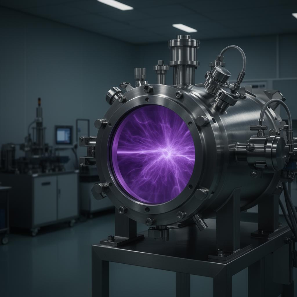
Pilot Series
Production-grade single-wafer tool with full SECS/GEM and recipe management — built for pilot fabs.
ConfigureBatch Series
High-throughput batch asher for volume photoresist strip in MEMS and compound semiconductor fabs.
ConfigureEngineered for the
processes that matter.
From university research benches to high-volume MEMS production lines, our systems are deployed across the full semiconductor lifecycle.
- 01Photoresist stripping
- 02Post-etch polymer removal
- 03Descum & via cleaning
- 04MEMS sacrificial release
- 05Surface activation
- 06Compound semiconductor
- 07GaN / SiC processing
- 08Wafer-level packaging
Tell us about your
process.
Every Forge Plasma system begins with a conversation about your chemistry, your wafer, and your throughput targets.